Purpose
The RT8130B is a high efficiency single phase synchronous Buck DC/DC controller with 5V/12V supply voltage. This document explains the function and use of the RT8130B evaluation board (EVB), and provides information to enable operation, modification of the evaluation board and circuit to suit individual requirements.
Introduction
General Product Information
The RT8130B is a high efficiency single phase synchronous Buck DC/DC controller with 5V/12V supply voltage. The RT8130B has embedded MOSFET gate driver with high driving capability, supporting driving voltage up to 12V for high output current application. This device uses lossless low-side MOSFET RDS(ON) current sense technique for over-current protection with adjustable threshold set by the LGATE pin (LGOCS). Other features include power good indication, enable/disable control and internal soft-start. The RT8130B also provides fault protection functions to protect the power stage output. With above functions, the IC provides customers a cost- effective solution for high efficiency power conversion. The RT8130B is available in the WDFN-10L 3x3 package.
Product Feature
-
High Light Load Efficiency
-
Single 5V to 12V Driver Voltage
-
Integrated High Driving Capability N-MOSFET Gate Drivers
-
300kHz Fixed Frequency Internal Oscillator
-
85% Maximum PWM Duty Cycle
-
Power Good Indicator
-
Enable/Disable Control
-
Internal Soft-Start
-
Lossless Low-Side MOSFET RDS(ON) Current Sensing for Over-Current Fault Monitoring
-
LGATE Over-Current Setting (LGOCS)
-
Dedicated Output Voltage Monitor
-
OCP, UVP, OVP, OTP, UVLO
Key Performance Summary Table
|
Key Features
|
Evaluation Board Number : PCB048_V1
|
|
Input Voltage Range
|
19V
|
|
Max Output Current
|
7A
|
|
Default Output Voltage
|
12V
|
|
Default Marking & Package Type
|
RT8130BGQW, WDFN-10L 3x3
|
|
Operation Frequency
|
Steady 300kHz at all loads
|
Bench Test Setup Conditions
Headers Description and Placement
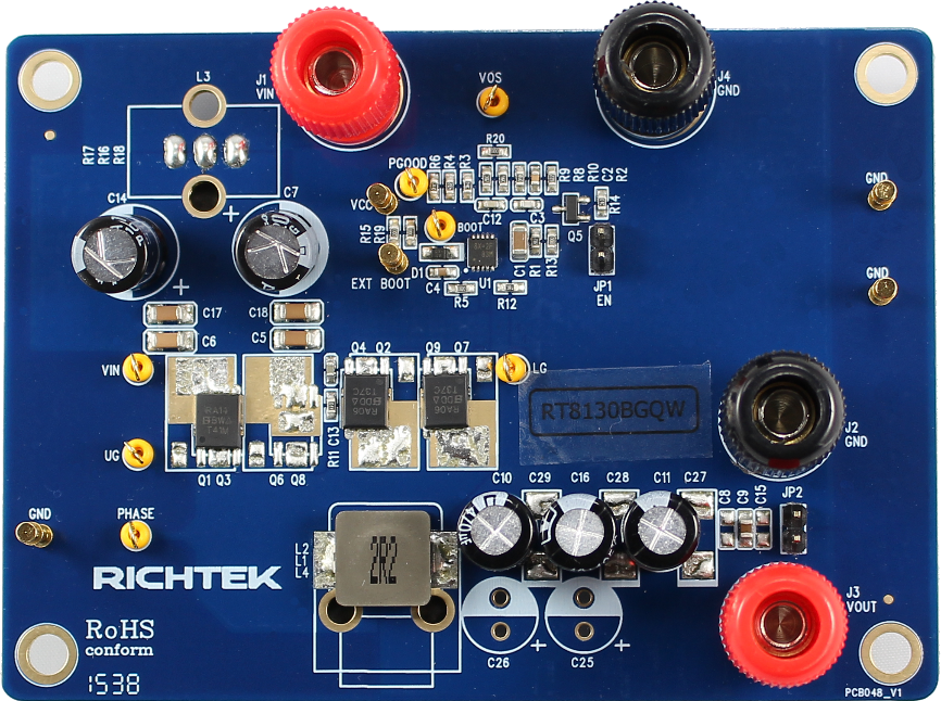
Please carefully inspect the EVB IC and external components, comparing them to the following Bill of Materials, to ensure that all components are installed and undamaged. If any components are missing or damaged during transportation, please contact the distributor or send e-mail to evb_service@richtek.com
Test Points
The EVB is provided with the test points and pin names listed in the table below.
|
Test point/
Pin name
|
Signal
|
Comment (expected waveforms or voltage levels on test points)
|
|
VIN
|
Input voltage
|
Power input. Support 2.5V to 21V Input Voltage. Must bypass with a suitable large ceramic capacitor at this pin.
|
|
VCC
|
Internal Driver voltage
|
5V or 12V bias input supply. Connect a 2.2µF capacitor to ground.
|
|
GND
|
Ground
|
Ground.
|
|
BOOT
|
Bootstrap supply test point
|
Bootstrap supply for high-side gate driver. Connect a 0.1µF ceramic capacitor between the BOOT and SW pins.
|
|
PHASE
|
Switch node test point
|
Connect this pin to an external L-C filter.
|
|
UG
|
High-Side MOSFET Gate Driver Output
|
Connect this pin to the Gate of high-side MOSFET for floating drive.
|
|
LG
|
Low-Side MOSFET Gate Driver Output
|
Connect this pin to the Gate of low-side MOSFET. This pin is also used for Over-Current Protection (OCP) threshold setting. Connect a resistor (ROCSET) from this pin to the GND pin to set the OCP threshold.
|
|
PGOOD
|
Power Good Indicator Output
|
This pin provides an open-drain output. Connect this pin to a voltage source through a pull-up resistor.
|
Power-up & Measurement Procedure
1. Connect input power (2.5V < VIN < 21V) to VIN test pin.
2. Connect positive end and negative terminals of load to VOUT and GND test pins respectively.
3. Connect 5V or 12V for VCC test pin.
4. Verify the output voltage (approximately 12V) between VOUT and GND.
5. Connect an external load up to 7A to the VOUT and GND terminals and verify the output voltage and current.
Output Voltage Setting
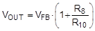
Set the output voltage with the resistive divider (R8, R10) between VOUT and GND with the midpoint connected to FB. The output is set by the following formula :
Schematic, Bill of Materials & Board Layout
EVB Schematic Diagram
Bill of Materials
|
Reference
|
Qty
|
Part Number
|
Description
|
Package
|
Manufacture
|
|
U4
|
1
|
RT8130BGQW
|
DC/DC Controller
|
WDFN-10L 3x3
|
RICHTEK
|
|
C1
|
1
|
1206X7R 2200nF
|
2.2µF/50V
|
X7R/1206
|
TDK
|
|
C2
|
1
|
0603X7R 4700nF ±10% 50V
|
4.7nF
|
X7R/0603
|
TDK
|
|
C3
|
1
|
0603NPO 82pF ±5% 50V
|
82pF
|
NPO/0603
|
WALSIN
|
|
C4
|
1
|
C1608X7R1H104KT000N
|
0.1µF/50V
|
X7R/0603
|
TDK
|
|
C5, C6, C17, C18
|
4
|
C3216X5R1H106KT000N
|
10µF/25V
|
X5R/1206
|
TDK
|
|
C7, C14
|
1
|
1206X7R 2200nF ±10% 50V
|
1000µF/25V
|
|
|
|
C9
|
1
|
C2012X5R1C106KTK0HN
|
10µF/16V
|
|
TDK
|
|
C10, C11, C16
|
1
|
|
470µF/16V
|
|
|
|
C12
|
1
|
|
820pF
|
C0603
|
WALSIN
|
|
C13
|
1
|
|
2.2nF
|
C0603
|
WALSIN
|
|
D1
|
1
|
1N4148_R1_00001
|
1N4148
|
|
RANJIT
|
|
L2
|
1
|
MMD-10DZ-2R2M-X1
|
2.2µH
|
|
Mag.Layers
|
|
Q1
|
1
|
SIRA14DP
|
|
|
VISHAY
|
|
Q2, Q7
|
2
|
SIRA06DP
|
|
|
VISHAY
|
|
Q5
|
1
|
2N7002
|
|
|
RANJIT
|
|
R1
|
1
|
|
2.2
|
R0603
|
|
|
R2
|
1
|
|
8.2K
|
R0603
|
|
|
R5, R7, R13, R15, R19, R20
|
6
|
|
0
|
R0603
|
|
|
R6, R14
|
2
|
|
10K
|
R0603
|
|
|
R8
|
1
|
|
14.3K
|
R0603
|
|
|
R9
|
1
|
|
3K
|
R0603
|
|
|
R10
|
1
|
|
1K
|
R0603
|
|
|
R11
|
1
|
|
1
|
R0603
|
|
|
R12
|
1
|
|
15K
|
R0603
|
|
|
R16, R17, R18
|
3
|
|
0
|
R0603
|
|
PCB Layout
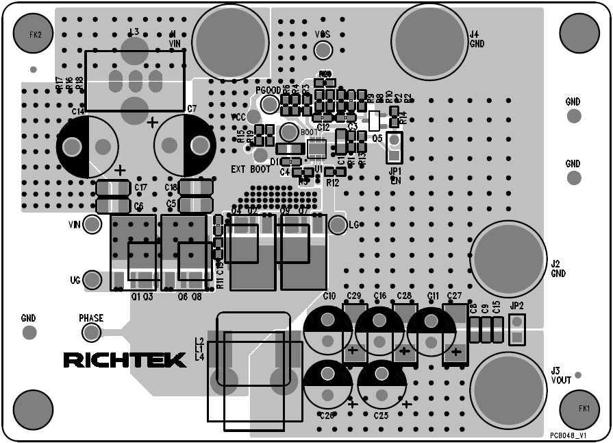
Top View (1st layer)

PCB Layout—Inner Side (2nd Layer)

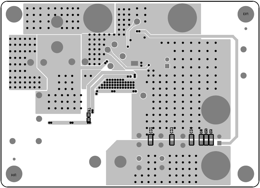
PCB Layout—Inner Side (3rd Layer)
Bottom View (4th Layer)